



DA9313-18 Charger IC – 10A Dual Cell Switched Capacitor
₨ 150
DA9313-18 Dual Cell Fast Charging IC
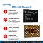
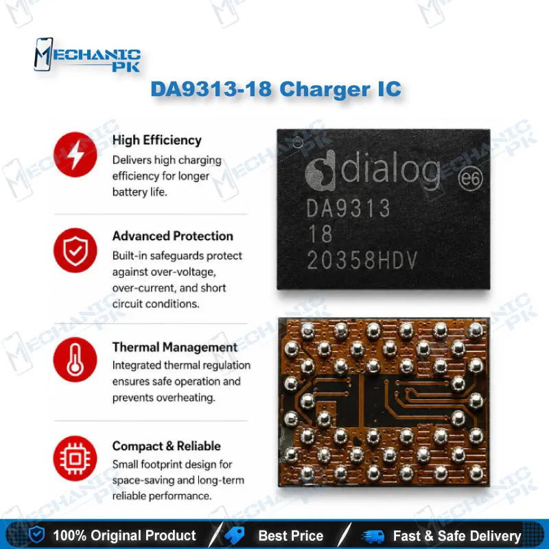
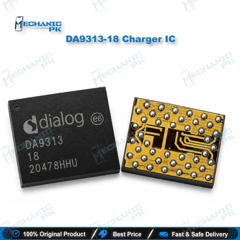
The DA9313-18 Charger IC is a Dialog Semiconductor switched capacitor divider built for smartphone direct charging and 2S Li-ion battery systems. It halves the input voltage through integrated power switches, needs no external inductor or FETs, and delivers up to 10A at up to 98% conversion efficiency across a 5.0V to 10.5V input range. Built-in over-temperature and over-current protection, programmable soft start, power good signalling, and I2C control make it a precise replacement for boards that show fast charging failure, heating on the charge path, or a short on the high-current rail. Match the full chip marking before you replace it.
DA9313 Charging IC for High-Current Fast Charging Boards
The DA9313-18 Charger IC belongs to Dialog Semiconductor’s DA9313 family, a high-efficiency dual cell switched capacitor divider that now sits in the Renesas portfolio. Mechanicpk supplies this DA9313 charging IC for technicians who handle board-level faults on fast-charging smartphones, where the main charger alone cannot carry the full charging current. The chip accepts any input between 5.0V and 10.5V, converts it at a fixed 2:1 ratio, and pushes up to 10A of output current with conversion efficiency reaching 98%. Two devices can run in master/slave mode and share the load for up to 20A. That combination makes it a core part of the high-power charging path, not a general-purpose regulator.
How the 2:1 Switched Capacitor Stage Works
Unlike a buck converter, the DA9313 uses flying capacitors instead of an inductor to divide the input voltage in half (VOUT = ½ VIN). Dialog integrated the pass devices on the die, so the board needs no external FETs and only low-profile capacitors around the chip. The design delivers more than 50W from a package under 10 square millimetres while keeping the thermal hotspot small. In a smartphone direct charging layout, the DA9313 works as a companion to the main charger IC. During the constant-current phase, it takes over the heavy current transfer and leaves precharge, termination and system power to the main charger. For a 2S stacked battery pack, it converts the pack voltage down to a single-cell level for the system rail. Because the output follows a fixed ratio of the input rather than a regulated value, a reading of roughly half the input on the output side tells you the stage switches normally. A reading far off that ratio points straight at the IC, its flying capacitors, or the enable signal.
Protection, Control and Fault Signs on the Board
The DA9313 carries integrated over-temperature and over-current protection, so it shuts down instead of burning the rail when a fault appears. A programmable soft start limits inrush current from the input node and brings the rail up on a controlled slope. Enable, low power mode, power good and nONKEY functions sit on configurable pins, and the host processor talks to the chip over I2C once it reaches ACTIVE mode. On the bench, these behaviours explain common charging issue complaints. A phone that charges only at normal speed, drops fast charging after a few seconds, or heats up around the charging section often has a DA9313 that trips protection or fails to start. A short to ground on the input or output rail, visible as instant current draw on a DC power supply, usually confirms a damaged chip. Check the front-end OVP IC as well, since board designs rely on that separate part for input over-voltage protection, and a charger surge often damages both together.
Replacing the DA9313 Charging IC on Your Bench
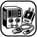
The chip comes in a 43-ball WLCSP package measuring 3.545 x 2.815 mm, so the job calls for controlled hot air, quality flux and a stable PCB holder. Pre-heat the board, lift the old chip without overheating the nearby flying capacitors, and clean the pads with solder wick before you place the new IC. Reballing with a fine stencil gives you even ball height on this dense array. Inspect alignment under a stereo microscope before reflow, then check the rails with a multimeter in diode mode for any remaining short. Always compare the full marking on the old chip with the replacement, because the DA9313 family ships in different factory-configured variants and the phone’s charging firmware expects the original one. After the IC change, test with the original fast charger and a USB power meter to confirm the phone negotiates high-power charging again. Pair this part with our Hot Air Stations, Reballing Kits, Microscopes and PCB Holders, and step up to a regulated DC power supply with current display when you diagnose charging faults every day.
| Weight | 0.1 kg |
|---|
Key Features
- 2:1 switched capacitor conversion with VOUT = ½ VIN
- Up to 98% conversion efficiency with flat efficiency across load
- 10A output current from a single chip
- Master/slave operation for up to 20A
- Inductor-less design with integrated pass devices, no external FETs
- Integrated over-temperature and over-current protection
- Programmable soft start with power good and enable control
- Compact 43-ball WLCSP package, 3.545 x 2.815 mm
Specifications
| Brand | Dialog Semiconductor (Renesas) |
|---|---|
| Model | DA9313-18 |
| Category | Charging IC / Power Management IC |
| Compatibility | Smartphones and devices with dual cell (2S) or direct charging architecture |
| Technology | 2:1 inductor-less switched capacitor divider, integrated power switches, I2C interface |
| Input Voltage | 5.0V – 10.5V |
| Output Voltage | ½ of input voltage |
| Power Rating | 10A output (up to 20A in master/slave mode), above 50W peak |
| Dimensions | 3.545 x 2.815 mm, 43-ball WLCSP |
Common Repair Uses
- Fast charging not working, phone charges only at normal speed
- Fast charging cuts off a few seconds after plugging in
- Short on the charging input or output rail
- Phone heating near the charging section during charging
- Charging section damage after a surge from a faulty charger
- Liquid damage repair on the high-current charging path
- IC change after output voltage fails the half-input ratio test
- Reballing and refitting during board-level charging repair
Compatible Devices
- Verified at architecture level — replace only on boards that carry the matching DA9313 marking
- Smartphones with dual cell (2S) stacked battery packs
- Smartphones using high-power direct charging
- Boards pairing the DA9313 with a main charger IC as a companion converter
- Devices with a 2:1 switched capacitor charging stage on a 5.0V–10.5V input
- Master/slave dual DA9313 layouts carrying up to 20A
- Portable devices powered by 2S Li-ion or Li-polymer packs
- Tablet and notebook designs built on 2S battery systems
- Any board where the original chip reads DA9313-18
FAQ
What is the product name?
What is the brand of this product?
What is the model of this product?
What is this product used for?
Which devices are compatible with this product?
Who should use this product?
Why does fast charging stop working when the DA9313 IC fails?
Does the DA9313 have built-in over-voltage protection?
Related products