





BN35 Charging iC – Mobile Phone Charging IC
₨ 300
BN35 Charging iC for Charging Circuit Repair
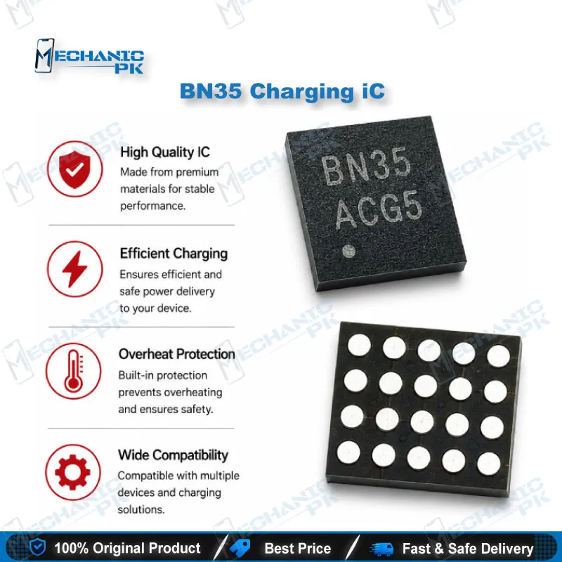
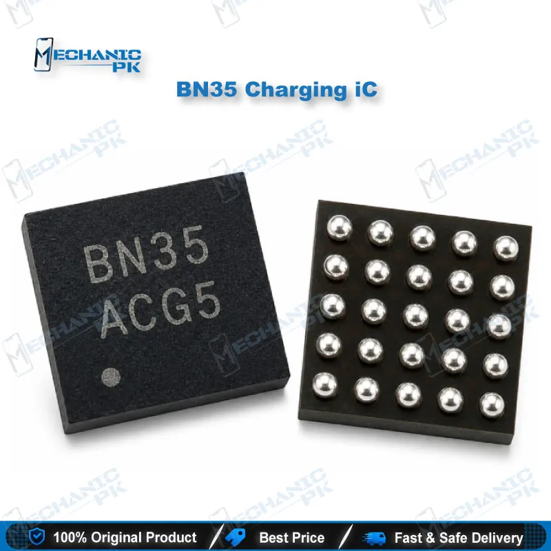
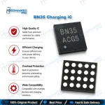
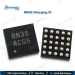
BN35 Charging iC is a 20-pin QFN power management IC marked BN35 on the package, and suppliers position it as a charging IC in budget Android handsets. It handles charging input, battery charge management, overvoltage protection, and circuit drive control. When a handset refuses to detect a charger, charges slowly, or dies after a short on the charging path, this chip is a common suspect. Replacement needs a hot air rework station, flux, and steady micro-soldering. Confirm the marking on the board before you order.
BN35 Charging iC is a surface-mount charging circuit IC in a 20-pin QFN package, and it sits in the USB charging path of budget Android phones. Its role covers battery charge management, overvoltage protection, and drive control for the charging circuit, so a fault usually shows up as no charger detection, slow charging, or a phone that will not power on after a short. Test the charging port, the battery connector, and nearby capacitors before you condemn this chip, because a shorted decoupling capacitor can mimic an IC failure. Once the fault is isolated, removal calls for a hot air rework station at a controlled temperature, fresh flux, and careful pad cleanup with solder wick. Reballing the chip before refitting gives cleaner seating on the pads, and checking for bridged pins under a microscope saves a second rework. Supplier listings disagree on which phone brands use this IC, so verify the device list against the board marking and schematic rather than assuming it. For a workshop, treat this as a board-level repair part that rewards careful process over speed.
| Weight | 0.1 kg |
|---|
Key Features
- Surface-mount QFN-20 package
- Marked BN35 on the chip
- Battery charge management function
- Overvoltage protection function
- Charging circuit drive control
- Suited to hot air rework stations
- Requires flux and micro-soldering skill
- Verify the board marking before fitting
Specifications
| Brand Entity | Not verified |
|---|---|
| Product Entity | BN35 Charging iC |
| Technology Entity | Charging management power IC, QFN-20 surface-mount package |
| Compatible Device Entities | Budget Android smartphones (brand scope not verified) |
| Repair Process Entity | Charging circuit IC replacement |
| Industry Entity | Mobile phone board-level repair |
Common Repair Uses
- Phone not detecting the charger
- Slow or intermittent charging
- Dead phone after a short on the charging path
- Charging IC replacement during board-level repair
- Isolating charging faults from decoupling capacitor shorts
Compatible Devices
- Budget Android smartphones with a USB charging circuit
FAQ
What is the product name?
What is this product used for?
Who should use this product?
Which devices are compatible with this product?
How do I confirm the BN35 is the right IC before replacing it?
Does this IC need a hot air station to replace?
Related products