









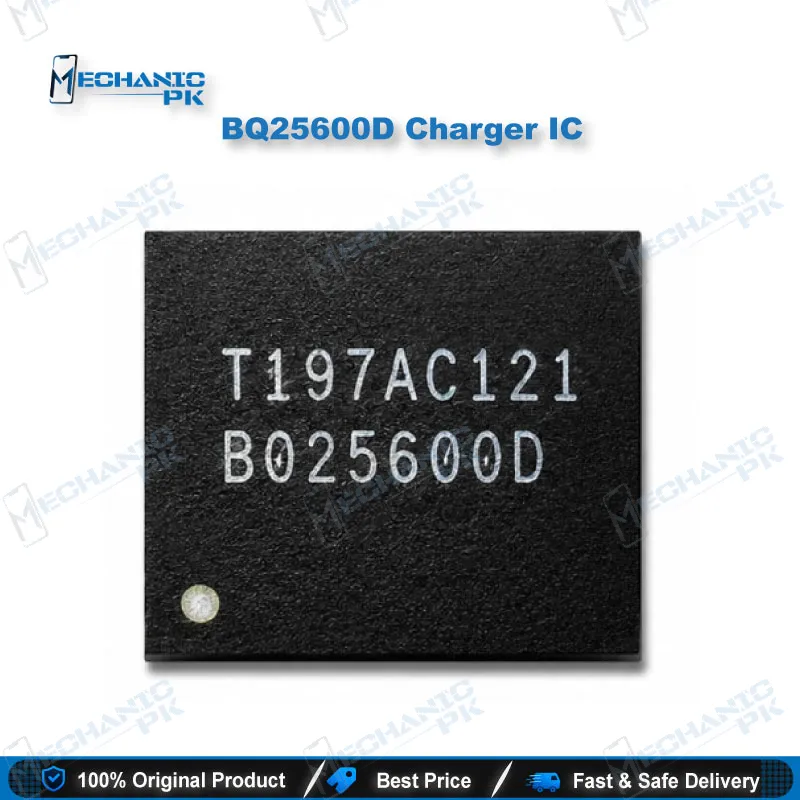
BQ25600D 3A Single-Cell Li-Ion Charger IC
₨ 480
Single-Cell Charging Control
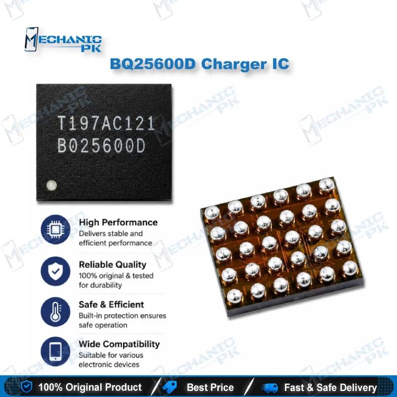
The BQ25600D is a 3 A, I2C-controlled buck charger for single-cell Li-ion and Li-polymer batteries. It combines a 1.5 MHz synchronous buck converter, NVDC power path management, and an input range of 3.9 V to 13.5 V with a 22 V absolute maximum rating. Its input current limit is programmable from 100 mA to 3.2 A in 100 mA steps, which covers USB 2.0, USB 3.0, and high-voltage adapters. The 30-ball DSBGA package suits board-level replacement work where a faulty charger stage is swapped out.
BQ25600D Charger IC: 3 A Single-Cell Buck Charger for Repair Benches
The BQ25600D charger IC is a 3 A, I2C-controlled buck charger for single-cell Li-ion and Li-polymer batteries. It targets handsets and tablets that need fast charging from high-voltage adapters as well as standard USB input. For a technician, the useful questions are where power enters the device, how the battery is regulated, and which symptoms point back to this stage. The sections below cover those points so the part can be matched to the right board position and checked on the bench.
BQ25600D Charger IC Power Path and Regulation
The device uses NVDC power path management, which keeps the system rail powered while the battery charges or sits discharged. A 1.5 MHz synchronous buck converter with integrated MOSFETs handles the conversion, so the board needs fewer external power stages. Charge voltage regulation holds within ±0.5 percent, and charge current regulation sits at ±6 percent at 1.38 A. Remote battery sensing improves accuracy at the cell during fast charge. Low battery leakage of 17 µA keeps standby drain small on a device resting on the bench.
Efficiency stays strong at the operating points that matter most. The converter reaches 92 percent charge efficiency at 2 A from a 5 V input. In OTG mode, the boost converter delivers up to 1.2 A with 92 percent efficiency at 1 A output. That gives the same device a second role when a board needs to power an accessory from its battery.
Input Range, Current Limits and Protection
The input range runs from 3.9 V to 13.5 V, with a 22 V absolute maximum rating that leaves headroom above the operating range. Input current limit is programmable from 100 mA to 3.2 A in 100 mA steps, so one design covers USB 2.0, USB 3.0, and high-voltage adapters. VINDPM can regulate the input voltage up to 5.4 V to extract maximum power from weak adapters. Thermal regulation reduces charge current when junction temperature passes 110 °C, and that threshold is programmable. A JEITA thermistor profile protects the battery during temperature extremes.
Detection logic matters on the bench too. The device integrates USB D+/D- and BC1.2 detection, which sets the input current limit according to the source type. Host mode and default mode behave differently, so the register state after power-up depends on how the host sets the registers. A handset that detects a USB source but refuses to charge points toward this input stage.
Where It Fits in a Charging Repair Workflow
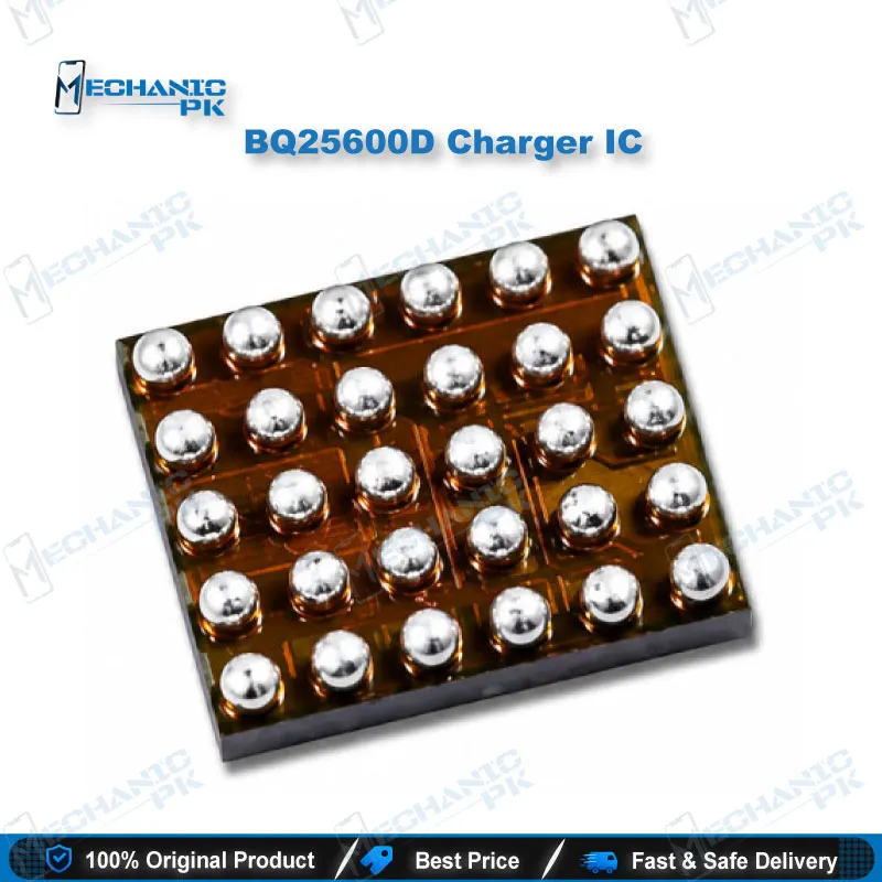
Start diagnostics at the input rail. Confirm VBUS arrives at the charger pins before you replace the IC. If the input is present and the battery still does not charge, move to the charge stage and the battery connector. A handset that charges slowly often points to input limit or thermal settings rather than a dead part. Use a multimeter for rail checks and a microscope to inspect the 30-ball DSBGA array for bridged or lifted balls.
Replacement is a precision job. The package measures 2.2 mm by 2.59 mm with 0.4 mm pitch and 0.375 mm thickness, so it needs a proper stencil, a controlled reflow profile, and inspection under magnification after removal. Check the PCB pads for lifted traces before reflow, and use PCB holders to keep the board flat under the hot air stream. After reflow, power the board, confirm the input path, and verify charge behavior before closing up the handset.
Build the bench around the work. Pair the rework with Hot Air Stations and Soldering Stations, use Reballing Kits for pad preparation, and rely on Multimeters and Microscopes for verification. Test Boxes help isolate the charge stage from the rest of the board, which speeds up fault tracing when the IC is one of several suspects.
| Weight | 0.1 kg |
|---|
Key Features
- 3 A maximum charge current with ±6% regulation at 1.38 A
- 1.5 MHz synchronous buck converter with integrated MOSFETs
- NVDC power path management for system rail support
- Programmable input current limit from 100 mA to 3.2 A
- Input range of 3.9 V to 13.5 V with 22 V absolute maximum
- USB OTG boost output up to 1.2 A
- JEITA thermistor monitoring with programmable 110 °C thermal regulation
- 17 µA low battery leakage current
Specifications
| Brand | Texas Instruments |
|---|---|
| Model | BQ25600D |
| Category | Battery Charger IC |
| Compatibility | Single-cell Li-ion and Li-polymer battery systems |
| Technology | I2C-controlled 1.5 MHz synchronous buck charger with NVDC power path management |
| Input Voltage | 3.9 V to 13.5 V operating, 22 V absolute maximum |
| Output Voltage | Battery charge voltage 3.85 V to 4.62 V |
| Power Rating | 3 A maximum charge current, 1.2 A maximum OTG boost output |
| Dimensions | 2.2 mm x 2.59 mm DSBGA package, 0.375 mm thickness |
Common Repair Uses
- Charge-stage and power-path work on single-cell handset boards
- Charging issue diagnosis where the charge stage is suspect
- IC change karna: board-level replacement of a faulty charger IC
- Power path checks on devices that run from an adapter but drain quickly
- Reflow and reballing work on the 30-ball DSBGA package
- OTG boost output verification on boards with a USB OTG fault
- Charge voltage checks against the 3.85 V to 4.62 V regulation window
- Input current limit checks for USB and adapter charging faults
- Fault isolation with multimeters and microscopes during board-level repair
Compatible Devices
- Single-cell Li-ion battery systems
- Single-cell Li-polymer battery systems
- USB 5 V input sources (USB 2.0 and USB 3.0 power specifications)
- High-voltage adapters in the 3.9 V to 13.5 V input range
- Designs requiring USB OTG boost output up to 1.2 A
- Designs using I2C host control for charge and input settings
- Batteries with thermistor monitoring under the JEITA profile
- Phone-model compatibility not verified; confirm board position before fitting
FAQ
What is the product name?
What is the brand of this product?
What is the model of this product?
What is this product used for?
Which devices are compatible with this product?
Who should use this product?
Does the BQ25600D support USB OTG?
What input voltage range does the BQ25600D accept?
Related products