











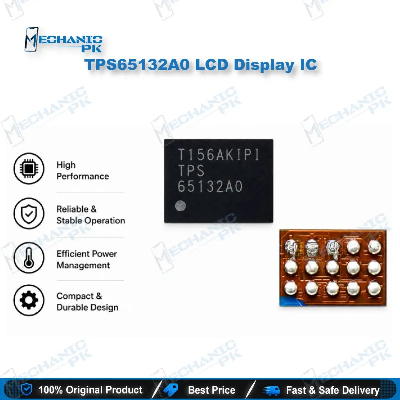
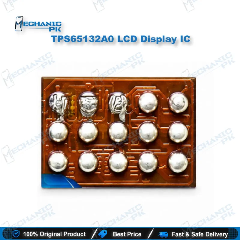
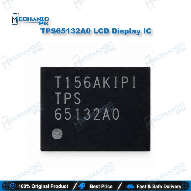
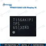
TPS65132A0 LCD Display IC – Dual Output LCD Bias Power
₨ 200
Dual Output LCD Bias IC for Compact TFT Displays
TPS65132A0 LCD Display IC generates a positive boost rail from 4 V to 6 V and a negative inverting rail from -6 V to -4 V from a single 2.5 V to 5.5 V input. Both outputs share one inductor, which keeps the bias section small and efficient. Each rail supports 80 mA or 150 mA output current depending on the option selected, with 1% voltage accuracy across the full temperature range. I2C control lets you set each rail voltage in 0.1 V steps, configure power-up and power-down sequencing, and enable programmable active output discharge.
TPS65132A0 LCD Display IC is a split-rail, single-inductor dual output power converter that supplies the positive and negative bias voltages required by small to medium TFT LCD panels. It operates from a 2.5 V to 5.5 V input, which covers a single Li-ion cell as well as regulated 3.3 V and 5 V rails common in phones and compact tablets. The boost stage produces VPOS between 4 V and 6 V in 0.1 V steps, while the inverting buck-boost stage produces VNEG between -6 V and -4 V in the same step size. Both rails share one inductor, so the converter keeps the external component count low and frees board space around the display flex connector. For a technician, this architecture matters during fault isolation, because a missing positive or negative rail points to a specific part of the power path rather than the panel itself. Each output supports either 80 mA or 150 mA, depending on the variant selected. Efficiency exceeds 85% at output currents above 10 mA and 90% above 40 mA, which keeps heat low inside a sealed phone enclosure. Output voltage accuracy holds at 1% across the full operating range from -40 °C to 85 °C. Control runs over an I2C interface, so you program each rail voltage, set power-up and power-down sequencing, and enable programmable active output discharge without changing external resistors. The part also includes programmable non-volatile memory with more than 1000x programming capability, so your settings persist across power cycles. Under-voltage lock-out and thermal protection guard the device during abnormal input conditions. The IC ships in a 15-ball CSP package, and TI also lists a 20-pin QFN option. On the workbench, this translates into a clear sequence: confirm input voltage at the converter pin, check that the boost and inverting rails reach their programmed levels, and verify that the enable and I2C lines are active before you suspect the panel. When a display shows no image or a flickering picture, the bias rails belong near the top of your checklist. Replacing a faulty TPS65132A0 requires hot air rework with controlled temperature and flux, careful pad cleaning, and accurate placement under a microscope, since the CSP footprint leaves little room for error. Reballing and reflow should follow the recommended profile for fine-pitch packages, and a bench power supply helps you verify the new IC before you reinstall the display. Pair this IC with a stable bench supply, a multimeter with fine probes, and a hot air station for clean removal. Mechanicpk supplies the tools that support this workflow, including hot air stations, soldering stations, multimeters, microscopes, reballing kits, and PCB holders. Each of these shortens rework time and lowers the chance of pad damage on a fine-pitch part. Accurate rail measurement saves more time than blind replacement, so measure first and replace only when the data confirms a fault.
| Weight | 0.1 kg |
|---|
Key Features
- Input range of 2.5 V to 5.5 V, suited to single-cell Li-ion and regulated 3.3 V or 5 V rails
- VPOS boost output adjustable from 4 V to 6 V in 0.1 V steps
- VNEG inverting buck-boost output adjustable from -6 V to -4 V in 0.1 V steps
- Single-inductor topology for both rails, reducing external component count
- 80 mA or 150 mA maximum output current options
- 1% output voltage accuracy over the full temperature range
- I2C control with programmable sequencing, active output discharge, and non-volatile memory
- Under-voltage lock-out and thermal protection
Specifications
| Model | TPS65132A0 |
|---|---|
| Category | LCD Drivers (Driver ICs) |
| Input Voltage | 2.5 V to 5.5 V |
| Output Voltage | VPOS 4 V to 6 V (0.1 V step); VNEG -6 V to -4 V (0.1 V step) |
| Output Current | 80 mA or 150 mA maximum |
| Interface | I2C |
| Supply Current | 700 µA maximum |
| Operating Temperature | -40 °C to 85 °C |
| Package | 15-ball CSP (DSBGA-15); 20-pin QFN option |
Common Repair Uses
- Diagnosing a missing positive or negative rail on a no-image display
- Measuring VPOS and VNEG output levels against their programmed values
- Verifying input voltage and enable signals before replacing the panel
- Replacing a faulty bias IC through hot air rework and reballing
- Checking I2C sequencing and programmed rail settings on a programmer
- Isolating flicker or dim display faults to the bias power section
- Confirming a replacement IC on a test box before reinstalling the display
Compatible Devices
- Small to medium bipolar LCD displays
- TFT-LCD panels up to at least 10 inch, per the manufacturer’s stated scope
- Smartphone-class LCD bias applications with 2.5 V to 5.5 V input
- Compact tablet displays requiring positive and negative source driver rails
- Universal at the panel level, not tied to a specific phone model
- Board-level replacement on display bias sections that use this IC
FAQ
What is the product name?
What is the brand of this product?
What is the model of this product?
What is this product used for?
Which devices are compatible with this product?
Who should use this product?
What are the VPOS and VNEG output ranges?
Does this IC support I2C control for sequencing?
Related products