

















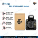
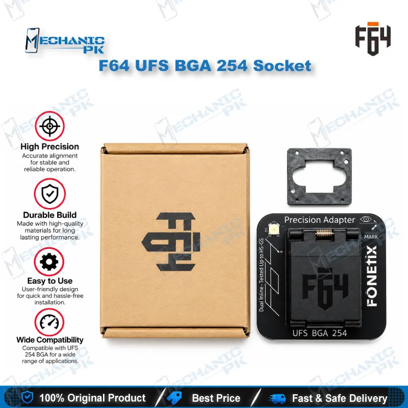
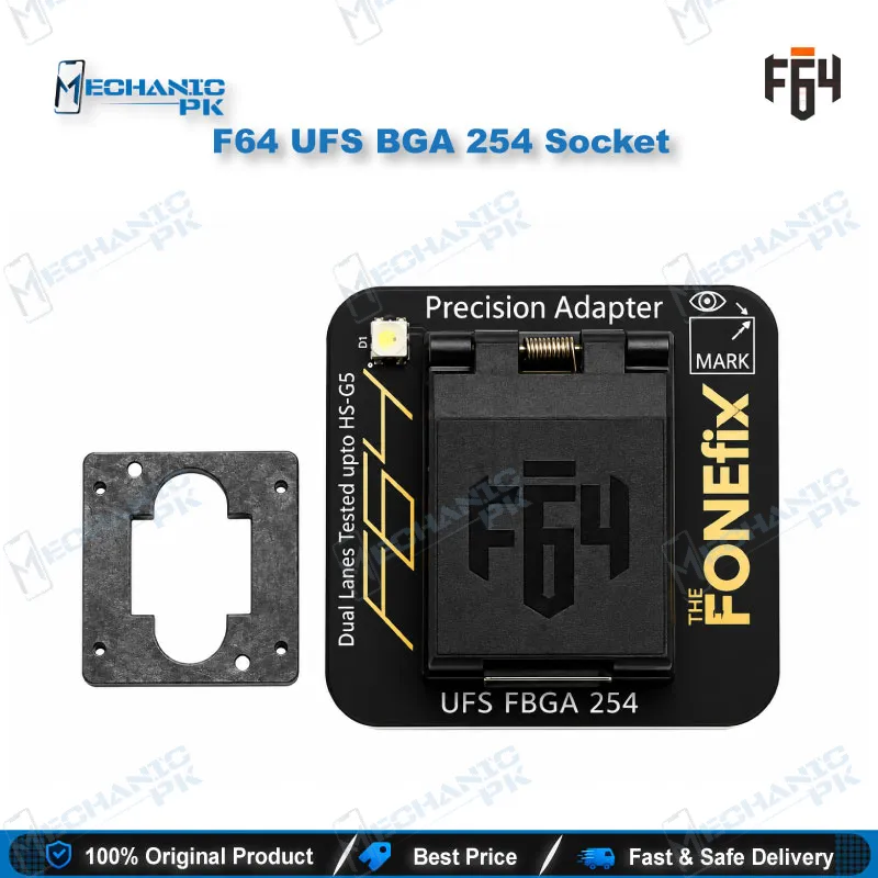
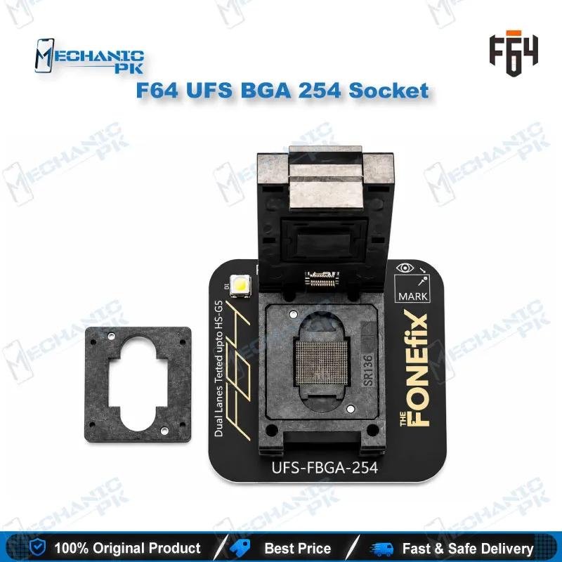
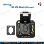
F64 UFS BGA 254 Socket Adapter for Flash64 Box
₨ 28,000
F64 UFS BGA 254 Socket for Direct UFS Chip Access
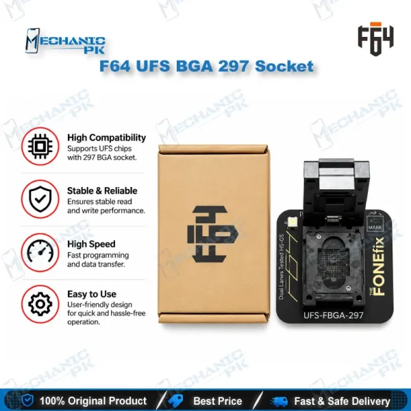
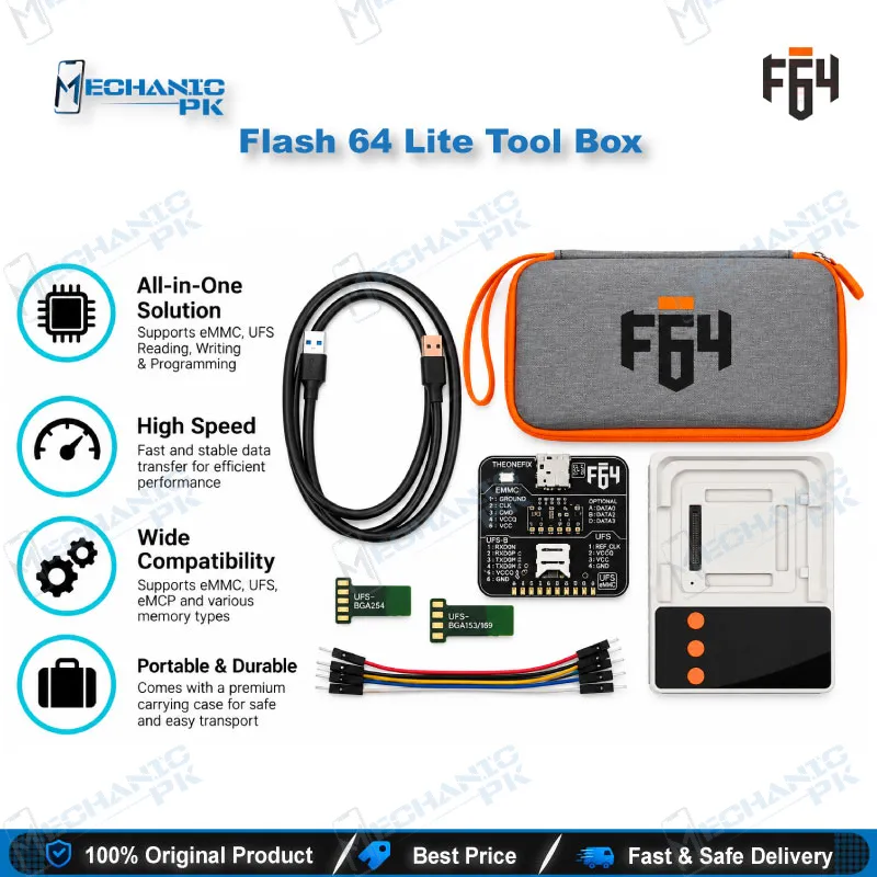
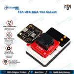
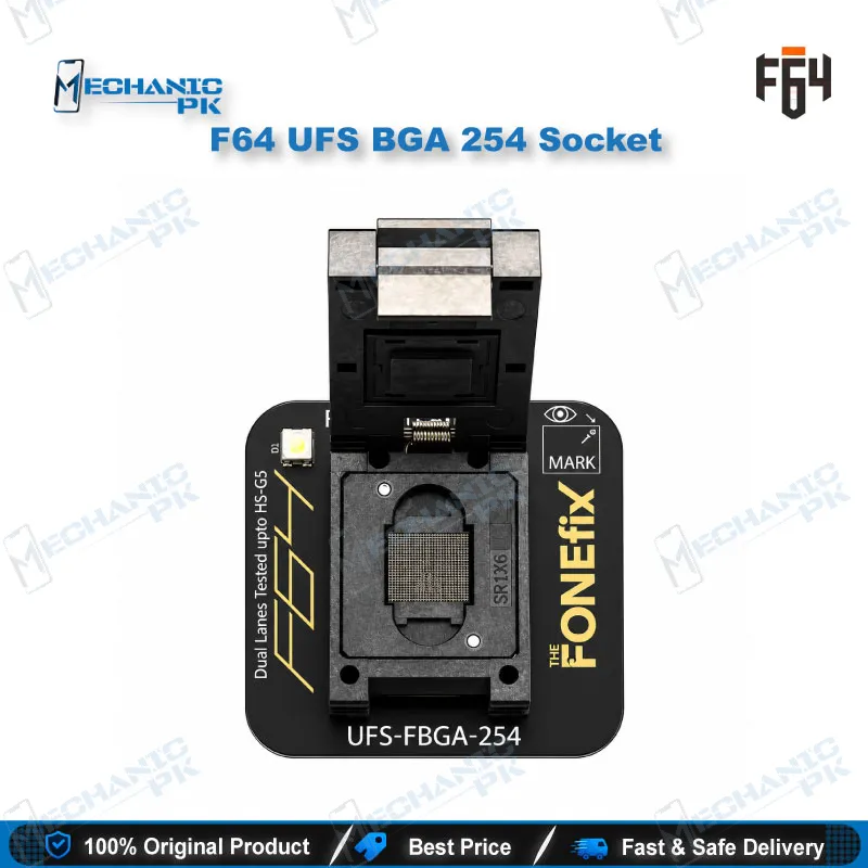
The F64 UFS BGA 254 socket connects UFS memory chips in the 254-ball package to your Flash64 setup without soldering the chip to an adapter board. You seat the removed IC in the socket, link it to your F64 box, and read or write the storage directly. The listed Flash64 family for this socket covers the F64 Box, F64 Lite JTAG, and F64 Ultra. You use it on dead phone cases, boot loop issues, and dead after flash faults where the UFS chip needs a direct check. Match the 254-ball count on your IC before you order, because BGA 153 and BGA 297 chips need their own sockets.
In stock
F64 UFS BGA 254 Socket for Chip-Off UFS Programming
The F64 UFS BGA 254 socket gives your Flash64 setup a direct, solder-free path to UFS memory chips in the 254-ball package. You drop a removed UFS IC into the socket, connect the adapter to your F64 box, and read or write the chip without fixing it to a board. Technicians use this route when a phone shows a dead phone symptom, a boot loop issue, or hang on logo after a failed flash, and the UFS storage itself needs a direct check. The socket suits shops that already run UFS-based Android repairs and want a repeatable bench method instead of improvised wiring. Mechanicpk supplies it as a package-specific adapter, so you match the socket to the ball count printed on your UFS IC before you order.
How the Socket Connects Your UFS Chip to the Flash64 Box
The socket mirrors the 254-ball layout of the UFS package, so each contact lines up with a solder ball on the underside of the chip. The F64 box supplies the programming interface and software, while the socket supplies the physical connection between the two. Because the chip sits in the socket rather than on a soldered adapter, you remove the soldering variable from every session. You also protect the IC from repeated heat cycles, which matters when the chip holds customer data or a unique device identity you cannot recreate. The socket targets the Flash64 family listed for it: the F64 Box, F64 Lite JTAG, and F64 Ultra. Confirm your box model before you buy, because sockets built for other programmer brands do not carry over.
Where It Fits in Your UFS Repair Workflow
You reach for this socket after diagnostics point at the storage chip. A typical sequence starts with a dead phone that draws normal current but never reaches the logo. You check the power rails, try the software route first, and move to hardware when software cannot reach the device. At that stage you lift the UFS IC with your hot air station, clean the pads and balls, and place the chip in the socket. From there you read the existing contents, write a corrected image, or prepare a replacement IC before IC change karna on the board. Technicians who run box chalana sessions daily value this order of work, because the socket turns a risky one-off job into a standard bench step.
Handling and Seating Practice for Reliable Contact
Contact quality decides whether your read finishes cleanly, so treat the seating step with care. Clean the chip balls with flux remover and inspect them under your microscope before you close the socket. Flat, evenly sized balls make better contact than worn or flattened ones, so reball the IC if it shows damage from removal. Align the chip to the socket markings, apply even pressure, and avoid sliding the IC across the contacts. Keep the socket free of flux residue and dust, and check the chip orientation twice before you start the session. If a read fails, reseat the chip first and inspect the balls again before you suspect the box or the software.
Choosing Between BGA 254, BGA 153 and BGA 297 Sockets
UFS chips ship in several ball-count packages, and each package needs its own socket. This F64 UFS BGA 254 socket covers the 254-ball package only. When your bench handles mixed devices, read the marking on each IC and pick the socket that matches its package before you plan the job. Many shops stock the 254 and 153 sockets together because both appear regularly in UFS repair work. If you want a fuller UFS kit, look at the multi-socket sets in our UFS Adapters category. For the surrounding bench, pair the socket with a Hot Air Station for chip removal, a Microscope for ball inspection, and a Reballing Kit for chips that need new balls. When your volume grows, a combined F64 Ultra setup gives you a clear upgrade path.
| Weight | 0.45 kg |
|---|
Key Features
- Socket layout for UFS chips in the 254-ball package
- Solder-free seating for repeatable chip-off sessions
- Listed for the Flash64 F64 Box, F64 Lite JTAG, and F64 Ultra
- Protects the IC from repeated heat cycles
- Direct read and write access to the UFS chip
- Suits dead phone and dead after flash recovery work
- Pairs with your hot air station, microscope, and reballing kit
- Separates cleanly from 153-ball and 297-ball sockets in your kit
Specifications
| Brand | F64 (Flash64) |
|---|---|
| Model | UFS BGA 254 Socket |
| Category | UFS Adapters |
| Compatibility | Flash64 (F64) Box, F64 Lite JTAG, F64 Ultra |
| Supported Devices | UFS memory ICs in the 254-ball FBGA package |
| Technology | UFS, FBGA 254 socket |
Common Repair Uses
- Chip-off UFS reading, writing, and preparation on the Flash64 platform.
- Recovering a dead phone caused by corrupted UFS contents
- Fixing dead after flash faults when software cannot reach the device
- Clearing a boot loop issue tied to damaged storage data
- Resolving hang on logo faults after the storage test points to the IC
- Reading UFS contents before IC change karna
- Preparing a replacement UFS chip before installation
- Testing a reballed UFS IC before you fit it back
- Checking a suspect UFS chip to confirm whether it or the board is faulty
Compatible Devices
- UFS ICs in the BGA 254 package, used with the Flash64 family. Model-level phone compatibility depends on the UFS chip fitted, so check the IC marking before use.
- UFS memory ICs in the 254-ball FBGA package
- Flash64 (F64) Box
- F64 Lite JTAG
- F64 Ultra
- UFS chips removed from dead phone mainboards
- Reballed UFS ICs awaiting a test read
- Replacement UFS ICs awaiting programming before installation
- Not for BGA 153 or BGA 297 chips, which need separate sockets
FAQ
What is the product name?
What is the brand of this product?
What is the model of this product?
What is this product used for?
Which devices are compatible with this product?
Who should use this product?
Can I use the F64 UFS BGA 254 socket on a BGA 153 or BGA 297 UFS chip?
Do I need to remove the UFS chip from the phone to use this socket for a dead phone?
Related products