





















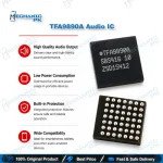
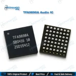
TFA9890A Audio IC | NXP Boosted Class-D Amplifier
₨ 350
NXP Boosted Class-D Speaker Amplifier IC
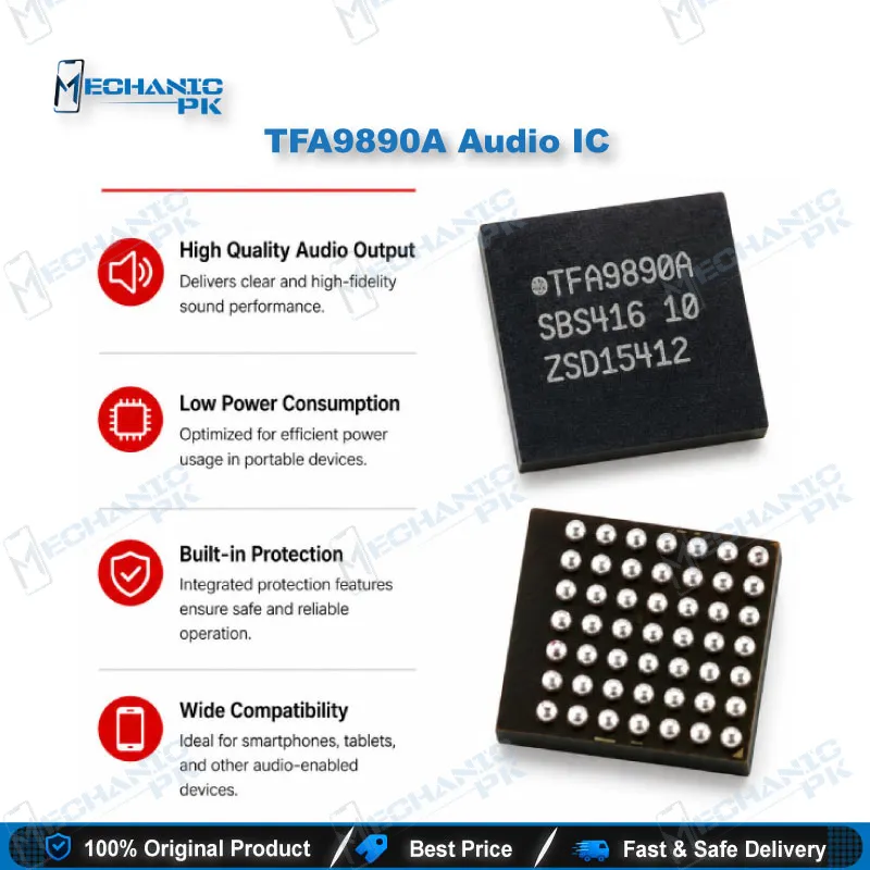
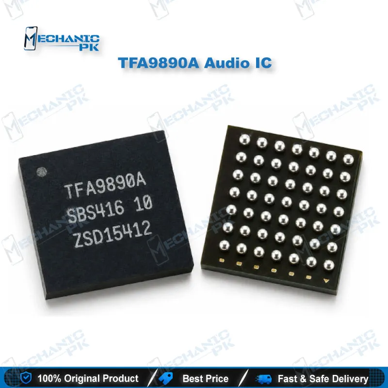
The TFA9890A is an NXP mono class-D audio amplifier IC with an internal boost stage and an adaptive sound maximizer. It drives a speaker in a bridge-tied load configuration and has distinct boost, mute and disabled operating states, which lets you isolate a speaker-path fault step by step. It comes in a 49-bump wafer-level package measuring 3.37 × 2.97 mm, so it suits board-level replacement where the speaker output has failed. This listing covers the single IC. Confirm the variant suffix against the original marking before ordering, because NXP ships several TFA9890 variants.
TFA9890A Audio IC for Board-Level Speaker Repair
The TFA9890A audio amplifier IC from NXP is a high-efficiency mono class-D device with a built-in boost converter. Its name refers to the 9.5 V boosted audio system, meaning the IC raises its internal supply when the battery voltage runs low and the speaker needs more headroom. For a technician, this explains why speaker output can change with battery level. This listing covers the standalone IC, supplied for replacement on the speaker output path of a board.
Key Technical Highlights
The device is a mono bridge-tied load (BTL) class-D amplifier. It pairs an adaptive sound maximizer with speaker protection, so it pushes more output while guarding the speaker against overload. The datasheet defines three operating states. Boost mode applies when the battery voltage is boosted. Mute mode keeps the output switching while the audio input is muted. Disabled mode applies when the class-D stage runs from an external supply instead of the internal boost. Knowing these states helps you tell a software-controlled mute from a real hardware fault on the output stage.
The IC uses a 49-bump WLCSP (wafer-level chip-size package) measuring 3.37 × 2.97 mm. Bump count and footprint matter at the bench. You need a reflow setup and a stencil or reballing method that matches this footprint before you attempt a replacement.
Where It Fits in the Speaker Repair Workflow
In a no-sound or weak-speaker complaint, check the speaker connector, the audio routing from the processor, and the supply rails before you suspect this IC. Once the supply is confirmed, the boosted rail and the output pins become the next checkpoints. A dead or shorted output stage, a damaged speaker path, or a fault that appears after a liquid damage repair on the audio section all point toward this amplifier.
Use a hot-air station with a controlled profile and quality flux for removal and placement. After replacement, verify the speaker output with a test tone and check the output under low-battery conditions before final reassembly. Retest in each operating state if the device still shows intermittent behavior.
Sourcing and Variant Checks
NXP lists several TFA9890 variants that differ by suffix and package status, and distributor records show different output power figures for each. Read the marking on the original component and match its suffix before you order. This listing does not state a supply voltage range or output wattage for this part, because those values change between variants. Check the NXP datasheet for the exact variant you plan to install. That step prevents mismatched replacements and keeps your repair records accurate.
| Weight | 0.1 kg |
|---|
Key Features
- Mono class-D BTL speaker amplifier
- Boosted 9.5 V internal supply system
- Adaptive sound maximizer with speaker protection
- Distinct boost, mute and disabled operating modes
- 49-bump WLCSP package, 3.37 × 2.97 mm
- Surface-mount board-level replacement
Specifications
| Brand | NXP |
|---|---|
| Model | TFA9890AUK |
| Category | Audio Amplifier IC |
| Compatibility | IC-level part for mono speaker output circuits |
| Supported Devices | Not device-specific; verify against the original board marking |
| Technology | Boosted class-D amplifier with adaptive sound maximizer and speaker protection |
| Channels | Mono (BTL) |
| Package | WLCSP49 (49 bumps) |
| Dimensions | 3.37 × 2.97 mm |
Common Repair Uses
- Typical board-level scenarios where this IC gets replaced or checked.
- Replacing a dead or shorted speaker amplifier IC on a no-sound board
- Diagnosing weak or distorted speaker output before replacing the speaker
- Checking the boosted supply rail when speaker volume drops on low battery
- Reflowing or reballing the 49-bump WLCSP after a board-level fault
- Restoring the speaker path after liquid damage on the audio section
- Confirming mute and disabled states during audio troubleshooting
Compatible Devices
- IC-level component; fitment is scoped to mono speaker output circuits using this footprint, not to a specific phone model.
- Mono BTL speaker output stages
- Boards using the TFA9890AUK 49-bump WLCSP footprint
- Boosted-supply audio designs (9.5 V boosted system)
FAQ
What is the product name?
What is the brand of this product?
What is the model of this product?
What is this product used for?
Which devices are compatible with this product?
Who should use this product?
What does the 9.5 V in the name mean?
What package is this IC supplied in?
Related products