






















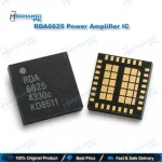
RDA6625 Quad-Band GSM Power Amplifier Module
RDA6625 Quad-Band GSM Module for Repair Benches
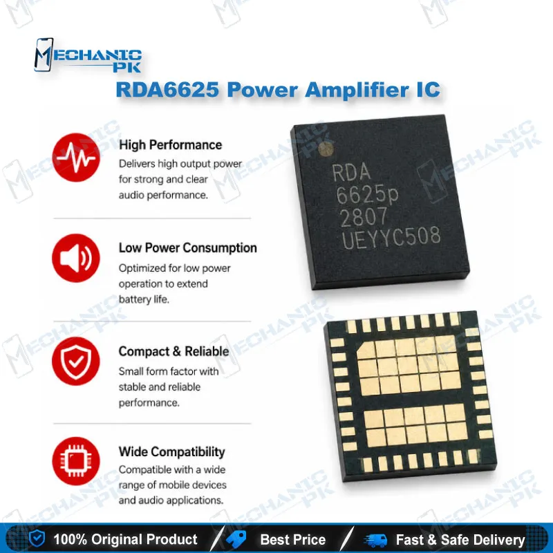
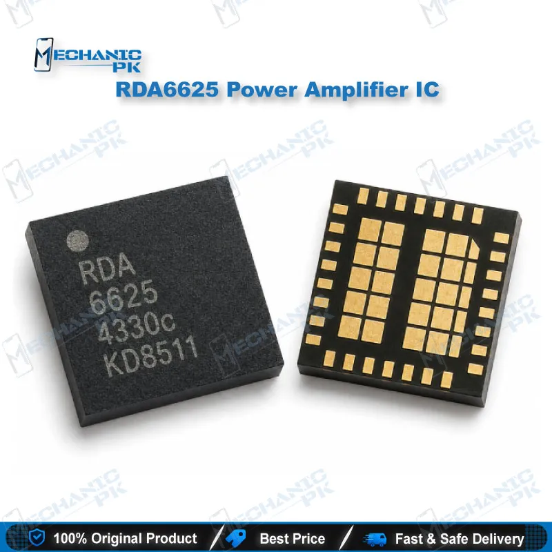
The RDA6625 combines quad-band GSM power amplifiers and an antenna switch in one compact 5 mm × 5 mm LGA module. It covers GSM850, EGSM900, DCS1800, and PCS1900, the four bands your handset transmit path depends on. The module matches its RF input and antenna ports to 50 ohms on-chip, so you need few external components around it. Its pin roles for RF inputs, antenna output, and control logic give you a clear path for tracing dead transmit and no-network faults on the bench.
RDA6625 Quad-Band GSM Module: Its Role in Your Repair Workflow
The RDA6625 quad-band GSM PA module handles transmit power and antenna switching for handsets working on GSM850, EGSM900, DCS1800, and PCS1900. On the board, this module sits between the baseband transmit path and the antenna. When a handset loses transmit power or network, the module belongs on your shortlist of suspects. Understanding its pin roles lets you test faster, confirm faults before desoldering, and avoid replacing good parts. Work through the signal path step by step, and the fault usually becomes clear.
Band Coverage and RF Signal Path
The module supports four GSM bands, and it splits them across two dedicated RF inputs. GSMIN takes the GSM and EGSM signal, while DCSIN takes the DCS and PCS signal. Both inputs feed the internal power amplifiers, and the amplified output leaves through the ANT port toward the antenna. The datasheet also lists RX2 and RX3 as receive ports on the same package. When you trace a no-network fault, first determine which input the signal reaches. If the low bands are dead but the high bands respond, concentrate your measurements on the GSMIN path. This split narrows the search to one section of the board and saves time on the bench.
Control Pins: TXEN, RAMP, CTR0, and CTR1
The control interface uses four signals. TXEN enables the transmitter, so you should check it first when the module stays silent in transmit mode. RAMP controls the output power ramp, which shapes the burst envelope to match GSM timing. CTR0 and CTR1 set the logic states that the internal control circuitry uses. Measure each line during power-on testing, then compare your readings with the reference schematic for that handset. Missing or incorrect control signals can produce dead transmit behavior even when the module itself is healthy. Verifying these pins before you order a replacement prevents unnecessary part swaps and wasted time.
Practical Use on Your Repair Bench
Start every session by confirming supply voltage on the VCC pins, which the datasheet lists at pins 13 and 14, along with a solid ground return through the GND pads. Then check the control lines and the RF input paths in sequence. If the module must be replaced, plan a controlled hot-air profile for this 32-pin LGA package and use quality flux to avoid bridging under the pads. Lift the module carefully, clean the pads, and reflow the new part at a controlled temperature. After replacement, retest transmit power and network registration on each band. Document your readings, because a consistent test routine improves your diagnosis on the next dead-phone job.
Key Features
- Quad-band coverage: GSM850, EGSM900, DCS1800, PCS1900
- Integrated antenna switch in one package
- GaAs HBT power amplifiers with CMOS control circuitry
- On-chip 50-ohm input and output matching
- Compact 5 mm × 5 mm × 1.1 mm 32-pin LGA package
- Control pins CTR0 and CTR1 for logic-level control
- TXEN enable and RAMP power-ramp control pins
- Separate GSMIN and DCSIN RF input ports
Specifications
| Brand | RDA Microelectronics |
|---|---|
| Model | RDA6625 |
| Category | Mobile Phone ICs |
| Compatibility | GSM850, EGSM900, DCS1800, PCS1900 handsets |
| Technology | GaAs HBT and CMOS |
| Dimensions | 5 mm × 5 mm × 1.1 mm, 32-pin LGA |
Common Repair Uses
- Restoring transmit power on quad-band GSM handsets after module failure
- Diagnosing no-network faults traced to the GSM or DCS RF path
- Checking TXEN and RAMP control lines during dead-transmit testing
- Verifying CTR0 and CTR1 logic levels during board-level fault finding
- Tracing antenna-side faults through the ANT port
- Replacing a faulty module on a hot-air rework station
- Confirming RX port continuity during receive-path checks
- Comparing GSMIN and DCSIN input paths to isolate band-specific faults
Compatible Devices
- Quad-band GSM handsets operating on the GSM850 band
- Handsets using the EGSM900 band transmit path
- DCS1800 band handsets with the DCS RF input path
- PCS1900 band handsets with the PCS RF input path
- Designs sharing this quad-band GSM front-end layout (confirm by board marking and schematic)
- Test setups covering 850, 900, 1800, and 1900 MHz GSM transmit
- Universal across quad-band GSM designs, not tied to one phone model
- Verify each handset schematic before fitting
FAQ
What is the product name?
What is the brand of this product?
What is the model of this product?
What is this product used for?
Which devices are compatible with this product?
Who should use this product?
Does the RDA6625 support GSM850 and PCS1900 bands?
What do the CTR0, CTR1, and TXEN pins do on the RDA6625?
Related products