









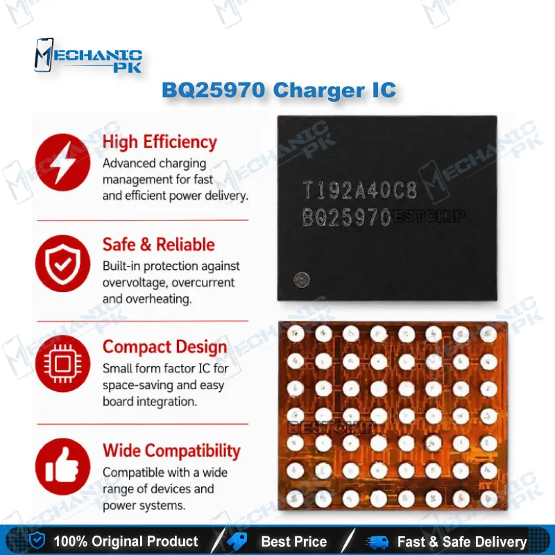
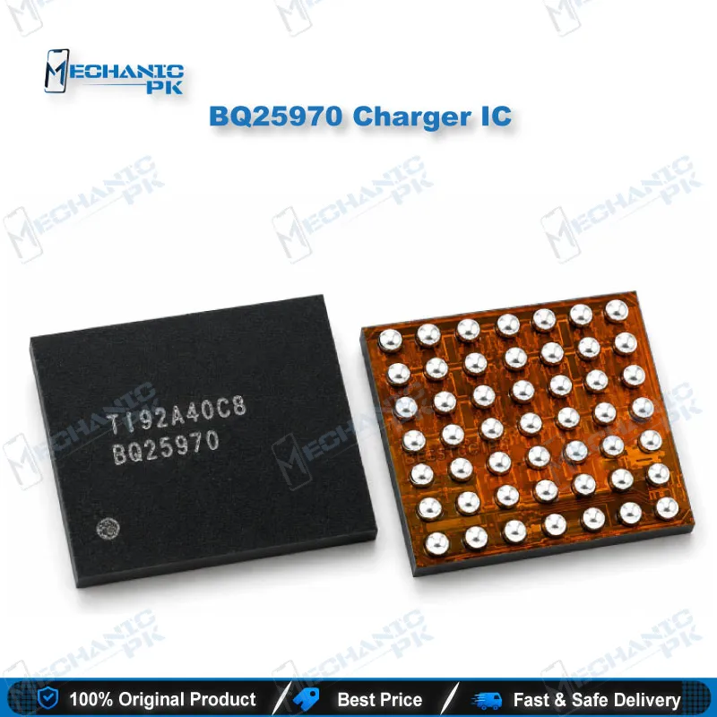
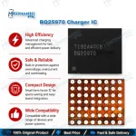
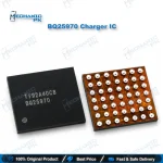
BQ25970 Charger IC 8A Switched Cap Fast Charger TI
₨ 1
8A Switched-Cap Fast Charging IC for Phone Board Repair
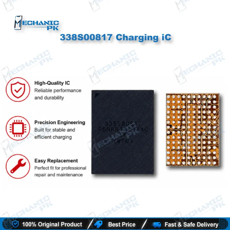
The BQ25970 from Texas Instruments is a single-cell, I2C-controlled switched-capacitor fast charger that pushes up to 8 A into the battery at roughly 97% efficiency. It sits beside the phone’s main buck charger and handles the high-current flash-charging stage, while the main charger covers pre-charge, CV, and termination. Mechanicpk supplies this 56-ball DSBGA part for technicians who trace a charging issue to the fast-charge section and need the exact IC for an IC change karna job, not a near-match substitute. Pair it with your hot air station, flux, and reballing stencil for a clean board-level replacement.
Out of stock
BQ25970 Charger IC for 8A Flash Charging Repair
The BQ25970 charger IC is Texas Instruments’ I2C-controlled, single-cell switched-capacitor fast charger, rated for up to 8 A of battery charge current at around 97% peak efficiency. Inside a smartphone, it never works alone. A conventional buck charger, such as a part from the BQ2589x family, handles pre-charge, the constant-voltage phase, and termination, while the BQ25970 takes over the high-current constant-current stage. That split matters at the repair bench: when a board charges on a normal adapter but refuses flash charging, the fault often lives in this stage. Mechanicpk stocks the genuine BQ25970 so you can replace the exact part your schematic calls for, without guessing at pin-similar alternatives.
How the 2:1 Switched-Cap Architecture Delivers 8 A
The BQ25970 runs a dual-phase charge pump at a fixed 50% duty cycle. The input sits at roughly twice the battery voltage, and the output current reaches twice the input current. With up to 4.5 A on the input side, the cable carries only half the current that reaches the battery, which cuts cable loss and keeps the phone cooler during fast charging. The interleaved dual-phase stage spreads power dissipation across both phases, lowers input capacitor requirements, and reduces output ripple.
Unlike a buck charger, this IC works as an open-loop charge pump. It relies on a smart wall adapter, typically USB Power Delivery with Programmable Power Supply (PPS), to adjust the input voltage in fine steps. That dependency explains a common field complaint: the phone charges fine on a generic adapter but drops to slow charging, because the flash stage only engages with a compatible PPS adapter and a healthy charge pump. TI rates the battery regulation range at 3.5 V to 4.65 V and the operating input range at 3.2 V to 12 V.
Protection Features and Fault Patterns on the Bench
TI packs a full protection set into this 8A switched cap charger IC. You get input overvoltage (BUS_OVP), input overcurrent (BUS_OCP) with an adjustable alarm, battery overvoltage (BAT_OVP), battery overcurrent (BAT_OCP), output overvoltage (VOUT_OVP), and a cycle-by-cycle current limit on the switching MOSFETs. It also monitors battery temperature, connector temperature, and its own die temperature. The integrated ADC reports these readings to the host over I2C, with STAT, FLAG, and MASK options for interrupts.
The BQ25970 also supports an external OVP FET on the VAC input, rated up to 17 V, plus optional VBATREG and IBATREG regulation when that FET is present. The sibling BQ25971 lacks both, so check your board design before treating them as interchangeable.
On the bench, a damaged fast charging IC for mobile usually shows up in a few ways. Flash charging stops while standard charging still works. A short on the input bus or battery output line pulls current the moment you connect power. In worse cases, a shorted part drags down the line and presents as a dead phone on the charger. Use your multimeter in diode mode on the bus and battery-side nets, then inspect for heat marks, cracked balls, or liquid corrosion under a microscope before you commit to rework.
BQ25970 Charger IC Replacement Workflow
The BQ25970 charger IC ships in a 56-ball DSBGA (YFF) package measuring about 3.0 mm × 3.6 mm, so treat it like any wafer-level BGA part. Lock the board in a PCB holder and shield nearby plastic connectors and small passives. Apply quality flux and lift the old IC with controlled hot air from your hot air station. Clean the pads with solder wick and a fine tip on your soldering station, then check every pad under magnification for lifted or torn copper.
Tin the pads or reball the new IC with a matching stencil from a reballing kit. Align ball A1 to the board marking, reflow with steady heat, and let the board cool without disturbance. Before you connect the battery, recheck the input and battery nets for shorts with your multimeter. Finish by testing with a PPS-capable adapter and watching for a proper jump in charging current.
For technicians who handle DSBGA charging ICs every day, a trinocular stereo microscope makes the natural upgrade from a basic bench magnifier. It speeds up ball alignment, pad inspection, and post-reflow checks on parts this small.
| Weight | 0.1 kg |
|---|
Key Features
- Up to 8 A battery charge current from a single IC
- Around 97% peak efficiency in the fast-charge stage
- 2:1 dual-phase switched-cap design that halves cable current
- Fixed 50% duty cycle with reduced output ripple
- Full protection set: BUS_OVP, BUS_OCP, BAT_OVP, BAT_OCP, VOUT_OVP
- External OVP FET support with VAC_OVP up to 17 V
- Integrated ADC with I2C reporting and interrupt flags
- Battery, connector, and die temperature monitoring
Specifications
| Brand | Texas Instruments |
|---|---|
| Model | BQ25970 |
| Category | Battery Charger IC (Switched-Capacitor Fast Charger) |
| Compatibility | Single-cell Li-Ion, Li-Polymer, and LiFePO4 batteries |
| Technology | 2:1 dual-phase switched-capacitor charge pump, 50% duty cycle, I2C control, integrated ADC |
| Input Voltage | 3.2 V – 12 V operating (20 V absolute max; VAC_OVP up to 17 V with external OVP FET) |
| Output Voltage | 3.5 V – 4.65 V battery regulation range |
| Power Rating | Up to 8 A charge current, up to 4.5 A input current, 97% peak efficiency |
| Dimensions | 56-ball DSBGA (YFF), approx. 3.0 mm × 3.6 mm |
Common Repair Uses
- Flash charging not working while normal charging still works
- Short on the input bus traced to the charge pump section
- Short on the battery-side output line during current testing
- Dead phone on charger caused by a shorted fast-charge IC
- Liquid-damaged charging section requiring an IC change
- Replacing an IC damaged by a faulty or unstable adapter
- Re-seating an IC with cracked solder balls after a drop
- Correcting a failed previous rework on the charging section
Compatible Devices
- Universal at the chipset level, not device-specific. Match the IC marking and footprint on the board before replacement.
- Single-cell Li-Ion and Li-Polymer smartphones with a 2:1 switched-cap fast-charge stage
- Boards that pair the BQ25970 with a main buck charger such as the BQ2589x family
- USB PD PPS-based flash-charging phone designs
- Boards using the BQ25970 in the 56-ball DSBGA (YFF) footprint
- Designs with an external OVP FET on the VAC input
- Single-cell LiFePO4 battery designs
- Systems controlling the charger over I2C from the host processor
- Designs with battery and connector thermistor monitoring
FAQ
What is the product name?
What is the brand of this product?
What is the model of this product?
What is this product used for?
Which devices are compatible with this product?
Who should use this product?
Can I use BQ25971 in place of BQ25970?
Why does the phone charge slowly instead of fast after a BQ25970 fault?
Related products