



DA9313-06 Charger IC – Dialog 10A Switched Capacitor Divider
₨ 150
DA9313-06 Dual-Cell Charging Power Stage
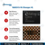
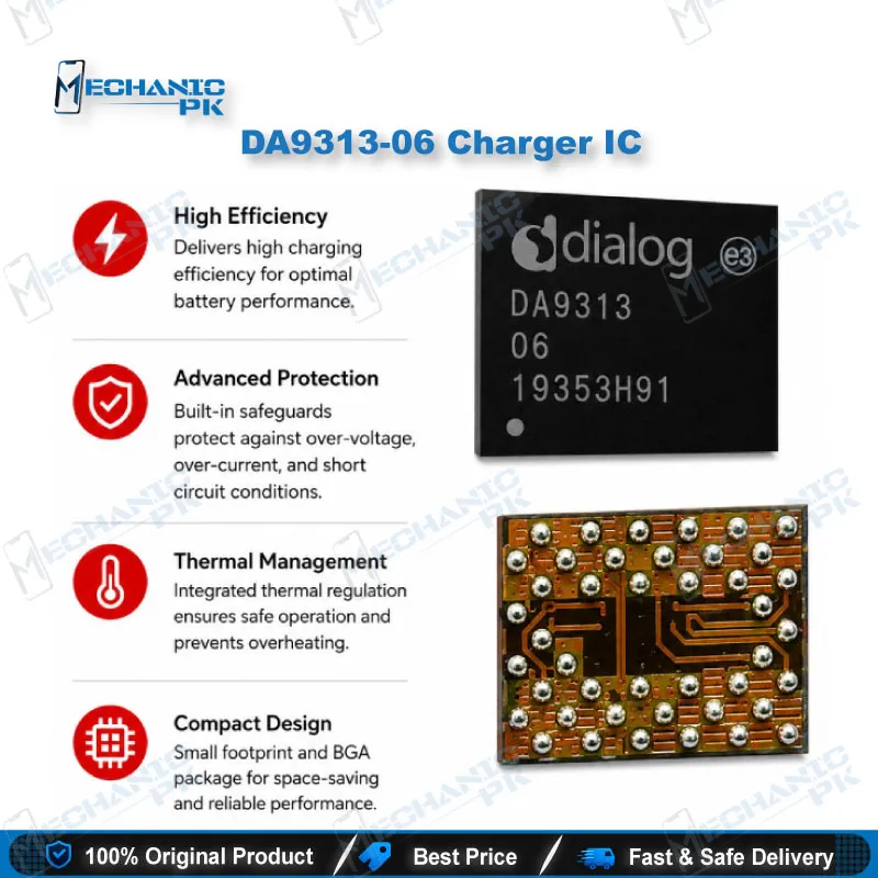
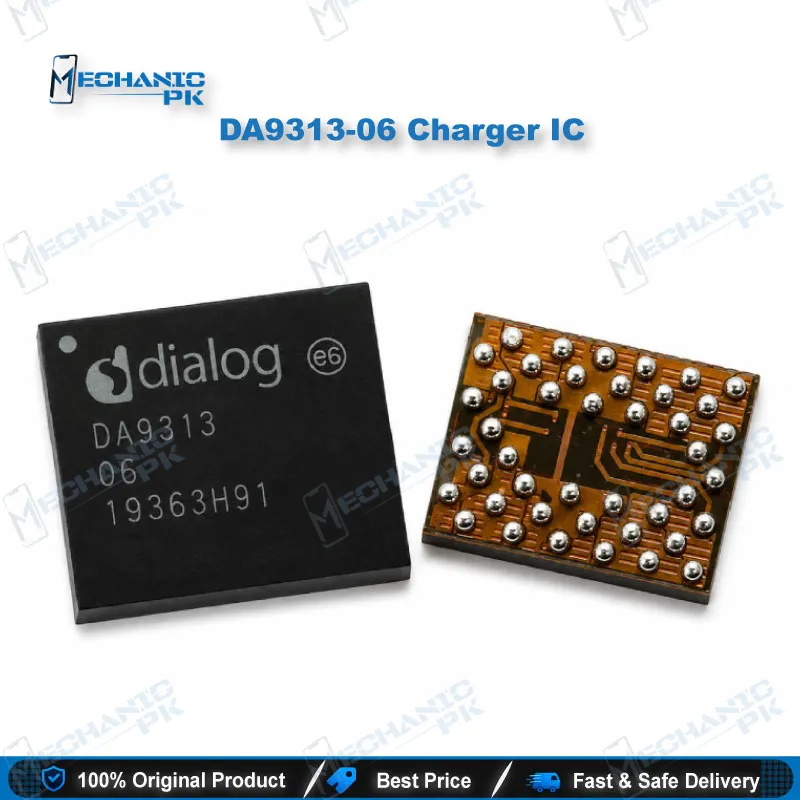
The DA9313 charger IC from Dialog Semiconductor (now Renesas) works as a 2:1 inductor-less switched capacitor divider for fast-charging smartphone boards. It accepts 5.0V to 10.5V, halves it, and delivers up to 10A at up to 98% efficiency inside a 43-ball WLCSP package that measures 3.545 x 2.815 mm. Phone makers use it on dual-cell (2S) battery designs and as a companion to the main charger IC in direct-charging paths. When this stage fails, you get a dead phone, a shorted charging rail, or fast charging that stops working. Match the full DA9313-06 marking before you replace the chip.
DA9313 Charger IC: Dialog’s 10A Inductor-less Power Stage for Fast-Charging Boards
The DA9313 charger IC from Dialog Semiconductor, now part of Renesas, is a 2:1 switched capacitor divider rather than a conventional buck charger. It takes any input between 5.0V and 10.5V and halves it without a single inductor, delivering up to 10A at conversion efficiency as high as 98%. Phone designers place it in two roles: on boards that run a dual-cell (2S) stacked battery, and in direct-charging paths where it carries the heavy constant-current phase. When this stage fails, the bench shows it quickly. You see high current draw on the DC power supply, a hot IC under rosin, or a dead phone with a short on the input rail.
How the 2:1 Divider Stage Works on the Board
The DA9313 integrates its pass devices on-die, so the circuit needs no external FETs. Its output tracks half of the input voltage and stays unregulated, which lets it feed system PMICs, sub-PMICs, and discrete regulators further down the power tree. The efficiency curve stays flat across a very wide current range, and Dialog rates it at more than 20% better efficiency than traditional buck regulators at light loads. Two chips can run as a master/slave pair and double the output to 20A, so some layouts carry two DA9313s side by side. In direct-charging designs, the main charger IC handles pre-charge and constant-voltage duties. During the high-power constant-current phase, the DA9313 bypasses the main charger and pushes 6A into the battery while staying inside the thermal budget. A programmable soft start limits inrush current from the input, and the chip also provides a power-good signal, an nONKEY input, and an I2C interface for control.
Diagnosing a Faulty DA9313 Before You Change the IC
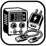
Confirm the fault before you touch the chip. Start with your multimeter in diode mode across the divider’s input and output rails and compare the readings against a known-good board. If the input rail reads near zero, power the board from the DC supply at a safe current limit and use rosin smoke or a thermal camera to find the hot component. A shorted DA9313 heats up fast, but a failed capacitor around the divider can mimic the same symptom, so lift suspect capacitors first. Check the USB and PD side and the main charger IC too, because a charging issue that starts upstream can look like a divider fault. If the phone charges slowly but refuses fast charging, the divider path is a strong suspect on direct-charging boards. This is a hardware fault, and no box or flash can fix it, so plan the repair as an IC change karna job from the start.
Replacing the DA9313-06: Rework Notes for WLCSP
The DA9313-06 sits in a 43-ball WLCSP, a bare-die package with no plastic shell to absorb heat mistakes. Lock the board in a PCB holder, apply a quality flux, and use a hot air station with a controlled airflow so you do not blow away the neighbouring capacitors. A preheater brings the board up gradually, which protects the PCB from pad lifting and limits stress on the underfill around nearby chips. After removal, clean the pads with solder wick and inspect them under a microscope before you seat the new chip. Dialog ships the DA9313 under several suffix codes (-02, -03, -04, -06 and others), so you get the right part only when the full marking on the replacement matches the original. Seat the IC, reflow, and verify the input and output rails with your multimeter before you connect a battery. For shops that handle charging-section repairs every day, a BGA rework station with bottom heating is the logical upgrade from a standalone hot air setup.
| Weight | 0.1 kg |
|---|
Key Features
- 2:1 inductor-less conversion that outputs half of the input voltage
- Up to 98% efficiency with a flat curve across a wide current range
- 10A output current, scalable to 20A in a master/slave pair
- 5.0V to 10.5V input range suits 2S battery packs and high-voltage charging inputs
- Integrated pass devices with no external FETs needed
- Programmable soft start limits inrush current at activation
- Built-in over-temperature and over-current protection, power-good output, nONKEY input, and I2C interface
- Compact 43-ball WLCSP package at 3.545 x 2.815 mm
Specifications
| Brand | Dialog Semiconductor (Renesas Electronics) |
|---|---|
| Model | DA9313-06 |
| Category | Mobile Phone ICs > Charging ICs |
| Compatibility | Dual-cell (2S) Li-ion/Li-polymer battery systems and smartphone direct-charging circuits |
| Supported Devices | Phone boards that carry the DA9313-06 marking |
| Technology | 2:1 inductor-less switched capacitor divider (VOUT = ½ VIN) |
| Input Voltage | 5.0V – 10.5V |
| Output Voltage | Half of the input voltage (unregulated) |
| Power Rating | 10A output; up to 20A in a master/slave pair; above 50W standalone |
| Dimensions | 3.545 x 2.815 mm, 43-ball WLCSP |
Common Repair Uses
- Board-level charging and power-rail faults involving the DA9313 stage
- Dead phone with a short on the DA9313 input rail
- High current draw on the DC power supply traced to a hot DA9313
- Fast charging fails while slow charging still works on direct-charging boards
- Phone heats up around the charging section during charging
- No power-up on 2S battery phones where the divider feeds the system PMIC
- Liquid-damage repair where corrosion has damaged the divider area
- IC replacement during full charging-section rework
Compatible Devices
- Circuit-level scope, not device-specific. Match the DA9313-06 marking on the original board.
- Smartphone boards with dual-cell (2S) stacked Li-ion or Li-polymer battery packs that use the DA9313
- Smartphone direct-charging circuits that pair the DA9313 with a main charger IC
- Any board that carries the DA9313-06 marking at the original position
- Battery-powered devices that run the DA9313 from a 5.0V–10.5V input rail
- Master/slave layouts that use two DA9313 chips (replace each with the same marking)
- Universal at IC level and not tied to a single phone brand or model
FAQ
What is the product name?
What is the brand of this product?
What is the model of this product?
What is this product used for?
Which devices are compatible with this product?
Who should use this product?
Can a faulty DA9313 cause a short on the charging line of a dead phone?
Can I replace a DA9313-06 with a DA9313-02 or DA9313-04?
Related products