





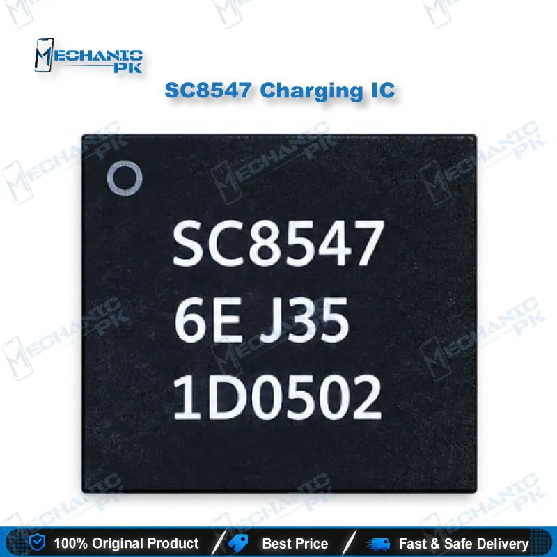
SC8547 Charging IC 6A Switched Capacitor Charge Pump
₨ 250
SC8547 Charging IC for Fast-Charge Repair
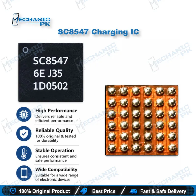
The SC8547 is a 6A switched capacitor charge pump that performs 2:1 conversion in fast-charge circuits. It accepts a 3V to 11V input and supplies a 3V to 5V output to the battery path, while its 50% duty-cycle operation keeps cable current near half the battery current. The CSP36 package needs controlled reflow and clean pads during replacement. Technicians turn to this part when voltage tracing points to the charge pump stage rather than the connector, PMIC, or battery.
SC8547 Charging IC: 2:1 Charge Pump Repair Reference
The SC8547 charging IC is a 6A switched capacitor charge pump from Southchip, and it sits in the fast-charge path where many charging faults begin. Its 2:1 topology converts voltage differently from linear or inductive designs, so your fault tracing needs a different approach. Many technicians replace the connector or battery first, and this stage often gets skipped. A short voltage check at the pump saves time and parts. This page covers the stated operating range, the CSP36 package, and the symptoms that point toward this IC. Use it as a reference when you plan a charging circuit repair or confirm a replacement part.
How the 2:1 Charge Pump Changes Your Fault Diagnosis
A 2:1 charge pump draws current from the adapter at about half the battery current, so cable and connector currents stay lower during fast charging. That behavior explains why the cable stays cooler on a healthy board. It also means a failed pump shows up as a voltage or current mismatch at the charge stage. Start with the adapter voltage at the input pins, then check the output at the charge pump pads, and finally the battery rail. A healthy input with a dead output points to the pump, while a dead input points upstream to the connector or protection circuit. Measure each stage with a multimeter and log the readings before you desolder anything.
CSP36 Replacement and Board-Level Handling
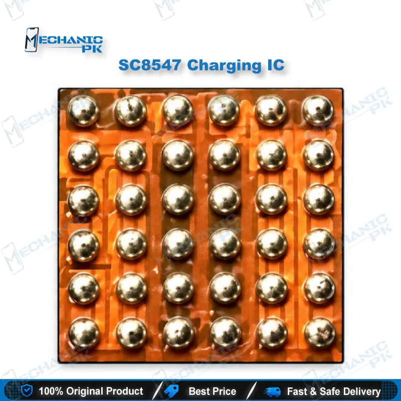
The SC8547 comes in a CSP36 package, so the pads sit under the body and you cannot inspect the joints visually. Clean the pads with flux and a fine tip before you place the new chip, and check for lifted traces under the microscope. Use a controlled reflow profile and keep the hot air nozzle moving so the board does not warp. Overheating the pad area can lift copper, and repeated reflow cycles raise that risk on a dense CSP footprint. Check the surrounding capacitors for heat damage after removal. After placement, verify the input and output rails again before you power the full board, and confirm the replacement part number matches the marking on the original chip.
Input Limits, Output Range, and Bench Checks
The stated input range runs from 3V to 11V, with an absolute maximum of 20V. Keep adapter voltages inside the operating range when you power the board on the bench. Use a current-limited supply set near the normal adapter voltage for your first power-up, and watch the current draw closely. The output range is 3V to 5V, which matches single-cell battery charging in most smartphones. The 6A figure works as a design ceiling rather than a bench target, because sustained high current heats the chip. The page states no bypass mode, so the chip operates only during active switched capacitor conversion. Record your readings after each power-up so you can compare them to the stated limits.
| Weight | 0.1 kg |
|---|
Key Features
- 6A rated switched capacitor charge pump for high-wattage fast charging
- 2:1 topology lowers cable current relative to battery current
- 50% duty-cycle operation with integrated FETs
- 3V to 11V input range with a 20V absolute maximum
- Compact CSP36 package for modern smartphone board layouts
- No bypass mode, so conversion occurs only during active charging
Specifications
| Brand | Southchip |
|---|---|
| Model | SC8547 |
| Category | Mobile Phone ICs, Charging IC |
| Technology | 2:1 switched capacitor charge pump |
| Package | CSP36 |
| Input Voltage | 3V to 11V (20V absolute maximum) |
| Output Voltage | 3V to 5V |
| Power Rating | 6A maximum output current |
| Weight | 0.01 kg |
Common Repair Uses
- Diagnosing no-fast-charge and slow-charge faults by tracing the charge pump stage
- Replacing a failed switched capacitor charge pump in a charging circuit
- Board-level CSP36 desoldering, pad cleaning, and reflow during charging IC swaps
- Recovering charging circuits after ESD or liquid damage, after the connector and battery test good
- Checking input and output rails after a charging IC replacement
Compatible Devices
- Charge-pump fast-charge circuits using the 2:1 switched capacitor architecture (chipset-family scope, not device-specific)
- Device-specific compatibility not verified; confirm against the target board’s schematic or boardview before installation.
- Confirm the replacement marking matches the original charging IC on the device.
FAQ
What is the product name?
What is the brand of this product?
What is the model of this product?
What is this product used for?
Which devices are compatible with this product?
Who should use this product?
What is the maximum output current of the SC8547?
Does the SC8547 support bypass mode?
Related products