










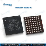
TFA9891 Audio IC NXP 9.5V Boosted Smart Speaker Amplifier
₨ 350
TFA9891 Audio IC for Loudspeaker Circuit Repair
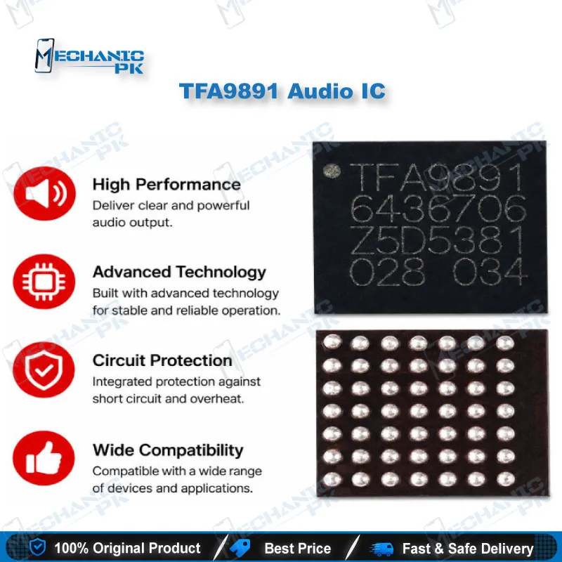
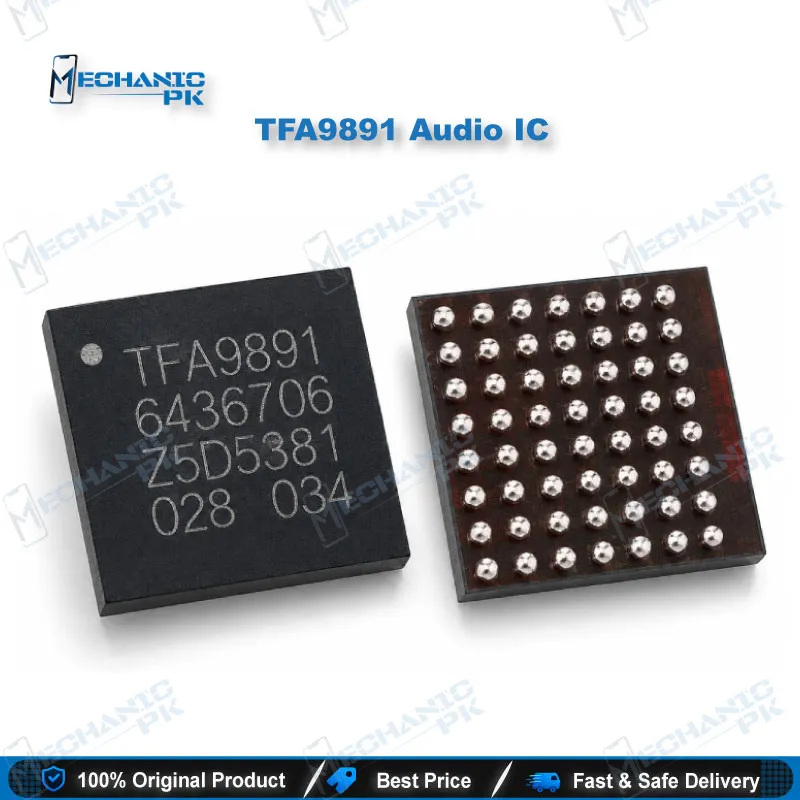
The TFA9891 Audio IC is an NXP smart speaker amplifier that combines a CoolFlux DSP, a mono class-D output stage, an adaptive 9.5 V boost converter, and speaker current sensing in one 49-bump WLCSP package. It drives an 8 Ω micro-speaker at up to 7.2 W peak from a 3.6 V battery and protects the speaker from overheating and over-excursion. Technicians replace it when a phone shows no loudspeaker sound, weak ringer audio, or distorted media playback while the earpiece still works. You get a genuine NXP part number for exact board-level replacement, backed by verified datasheet specifications for confident rail checks and fault diagnosis.
TFA9891 Audio IC: NXP’s Boosted Smart Amplifier for Phone Loudspeakers
The TFA9891 audio IC from NXP Semiconductors packs a CoolFlux DSP, a mono class-D amplifier, an adaptive DC-to-DC boost converter, and speaker sensing circuitry into a single wafer-level chip. Phone makers place it between the processor’s digital audio bus and the loudspeaker, where it lifts a 3.6 V battery rail to 9.5 V and pushes an 8 Ω micro-speaker to 3.6 W RMS at 1% THD, with 7.2 W available on peaks. When a handset arrives with a dead loudspeaker, low ringer volume, crackling media audio, or a speaker that cuts out at high volume, this chip belongs on your diagnosis list. Mechanicpk supplies the TFA9891 audio IC for technicians who handle board-level audio faults and need the exact NXP part instead of a loose substitute.
How the NXP TFA9891 Smart Amplifier Protects the Speaker
The NXP TFA9891 smart amplifier runs a SpeakerBoost algorithm built on an adaptive loudspeaker model. That model predicts membrane movement in real time and holds excursion within 10% of the rated limit, while direct measurement keeps voice coil temperature within 10 °C of its limit. A multiband dynamic range compressor controls up to three frequency bands independently, and clip avoidance prevents distortion even as the battery voltage sags. At low battery levels, the chip trims gain automatically so the audio system never pulls enough current to trigger a system undervoltage. An optional bandwidth extension mode stretches low-frequency response for fuller music playback. The model also adapts to speaker box leakage and thermal changes, so the protection stays accurate across different enclosures.
Interfaces and Rails That Matter During Diagnosis
Understanding the pin functions saves real bench time. The chip accepts audio through two selectable I2S inputs or one PDM input, uses a third I2S input for inter-chip communication, and takes its control commands over a 400 kHz I2C bus. Pins ADS1 and ADS2 set four separate I2C addresses, which lets stereo phones run two amplifiers side by side, so always check whether your board carries one chip or a pair. The digital core runs on a 1.8 V VDDD rail (1.65 to 1.95 V), while VBAT accepts 2.7 to 5.5 V. The I2S bit clock drives the DSP, the amplifier, and the boost converter together, and the chip needs both the bit clock and word select signals present to run. A missing 1.8 V rail or an absent audio clock produces the same “no speaker sound” symptom as a failed chip, so measure these before you decide on an IC change. The boost converter drops into follower mode when output demand stays below battery voltage, which means an idle BST rail reads close to VBAT rather than 9.5 V. The bridge-tied OUTA and OUTB outputs drive the speaker without an external filter and withstand short circuits across the load and to the supply lines.
Replacing the TFA9891 Audio IC on a Phone Board
The TFA9891 audio IC ships in a WLCSP49 package measuring 3.43 × 2.98 × 0.56 mm with a 0.4 mm bump pitch, and all NXP WLCSP parts use lead-free bumps. That fine pitch demands a controlled hot air process and a proper microscope. Heat the area until every joint melts fully, then lift the old chip with plastic tweezers, since metal tips can crack the bare silicon. Clean all solder and flux residue from the pads, apply flux to both the pads and the chip bumps, and use a flux-only placement rather than adding fresh solder. Align the new chip under magnification and reflow with a lead-free profile. NXP advises against reusing a removed chip because removal damages most of its bumps, so always fit a fresh part. A stable PCB holder, a quality hot air station, and a multimeter for rail checks complete the bench setup, and a stereo microscope upgrade makes 0.4 mm alignment far more reliable. Respect the moisture sensitivity precautions on the packing until you mount the chip.
| Weight | 0.1 kg |
|---|
Key Features
- Integrated CoolFlux DSP, class-D amplifier, boost converter, and current sensing in one chip
- Adaptive boost raises supply to 9.5 V only when the audio signal needs it
- 3.6 W RMS into 8 Ω at 3.6 V (1% THD), 7.2 W peak output
- Real-time excursion and voice coil temperature protection
- Multiband dynamic range compressor with up to three bands
- Battery protection reduces gain at low voltage to prevent undervoltage
- Two I2S inputs or one PDM input, plus 400 kHz I2C control with four selectable addresses
- 15 kV system-level ESD protection on the speaker without external parts
Specifications
| Brand | NXP Semiconductors Model: TFA9891 (TFA9891UK) |
|---|---|
| Category | Audio Amplifier IC / Smart Speaker Amplifier |
| Compatibility | Boards designed with the TFA9891 WLCSP49 footprint Supported |
| Devices | Mobile phones, tablets, notebooks, portable media players, small audio systems |
| Technology | Mono BTL class-D amplifier, CoolFlux DSP, adaptive DC-to-DC boost, I2S/PDM audio input, I2C control, WLCSP49 package with 0.4 mm pitch Input Voltage: 2.7–5.5 V (VBAT), 1.65–1.95 V (VDDD, 1.8 V typical) Output Voltage: Boosted supply up to 9.5 V Power Rating: 3.6 W RMS into 8 Ω at 3.6 V (1% THD), 7.2 W peak Dimensions: 3.43 × 2.98 × 0.56 mm |
Common Repair Uses
- Loudspeaker gives no sound while the earpiece works normally
- Ringer and notification volume is very low or missing
- Media playback crackles or distorts at high volume
- Speaker sound cuts out or drops during loud playback
- No loudspeaker audio on speakerphone calls
- Replacing a burnt or physically damaged amplifier after liquid damage
- Short on the boost (BST/VDDP) rail traced to the amplifier
- Donor-free audio section rebuild using a fresh chip
Compatible Devices
- Universal at footprint level — fits any board that specifies the TFA9891; confirm the chip marking or schematic before replacement
- Smartphones whose loudspeaker circuit uses the TFA9891
- Stereo-speaker phones running two TFA9891 chips on separate I2C addresses
- Tablets with TFA9891-based speaker amplification
- Notebooks and netbooks with an 8 Ω micro-speaker design
- Portable media players and MP3 players
- Portable navigation devices
- Small audio systems built around the TFA9891
- Platforms that deliver audio over I2S or PDM with I2C control
FAQ
What is the product name?
What is the brand of this product?
What is the model of this product?
What is this product used for?
Which devices are compatible with this product?
Who should use this product?
What voltages should I measure around the TFA9891 when the phone loudspeaker is dead?
Can I reuse a TFA9891 removed from a donor board?
Related products