




























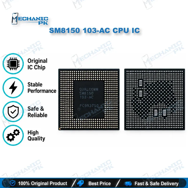
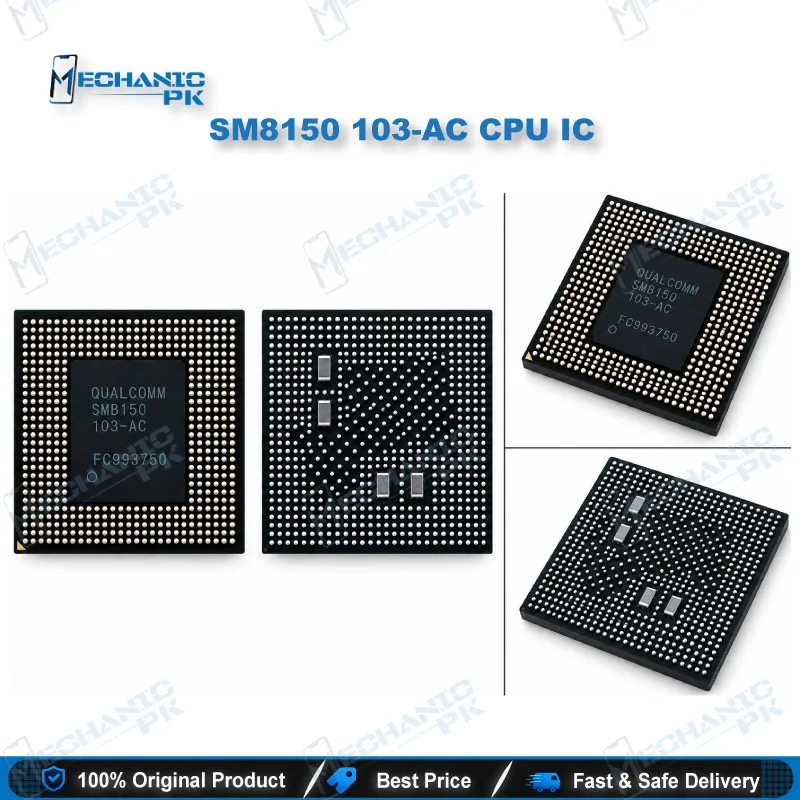
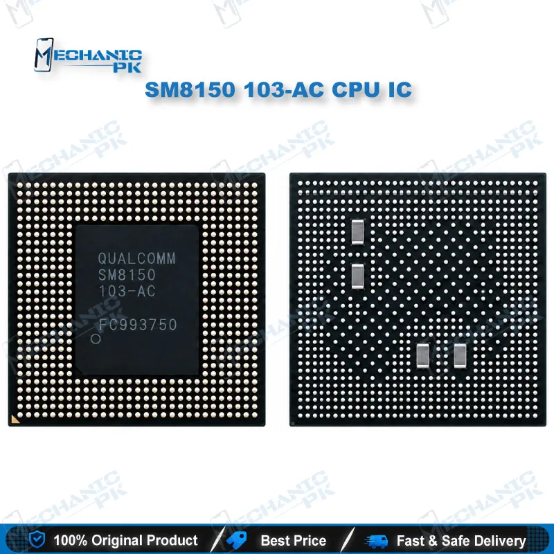
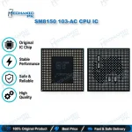
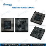
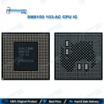
SM8150 103-AC CPU IC for Mobile Repair
₨ 6,600
SM8150 CPU IC Overview for Mobile Repair Technicians
The SM8150 is the Snapdragon 855 application processor from Qualcomm, manufactured on a 7 nm process. It pairs one 2.84 GHz prime core with three 2.42 GHz performance cores and four 1.78 GHz efficiency cores. The Adreno 640 graphics engine runs at 585 MHz, while the Hexagon 690 DSP handles offloaded signal and sensor tasks. For your repair bench, this IC matters most during board-level diagnosis, CPU reballing, and replacement on flagship Android phones built on this platform. Confirm the power rails and clock inputs first, then decide whether the fault sits in the processor itself.
SM8150 CPU IC Role in the Snapdragon 855 Platform
The SM8150 CPU IC sits at the center of the Qualcomm Snapdragon 855 platform, which launched in late 2018 and reached a wide range of flagship Android phones in 2019. Knowing how this processor is organized lets you read a fault correctly before you pick up the hot air station. Its eight Kryo 485 cores divide work between high-performance and efficiency clusters. The surrounding blocks handle graphics, digital signal processing, and memory access, and each one leaves its own trace on the board. Your diagnostic path should begin with the supply voltages and clock inputs feeding this IC. Only after those checks pass should you condemn the CPU and move toward reballing or replacement.
Kryo 485 Core Cluster Behavior
The Kryo 485 cluster uses a three-tier layout with one prime core at 2.84 GHz, three performance cores at 2.42 GHz, and four efficiency cores at 1.78 GHz. The prime core absorbs short, heavy bursts such as app launches and peak benchmark loads. The performance cores sustain multitasking, and the efficiency cores carry background services that keep an idle handset from draining its battery. When a unit throttles early or drops cores on your bench test, compare its frequency behavior against these reference values. Persistent clock drops under light load can point toward a thermal or power issue on the board, so inspect the surrounding components before you blame the die.
Graphics, DSP, and Memory Interface
The Adreno 640 GPU operates at 585 MHz and supports output up to 3840 x 2160 pixels. The Hexagon 690 DSP takes audio, sensor, and other signal tasks away from the main cores, which can reduce load during camera and media use. Memory connects through an LPDDR4X interface, so the memory package and its routing must match the original board design during any service. After a CPU replacement, check the memory rails and data lines if the unit shows display faults or fails to complete boot. Always reference the exact board revision, because trace layouts and supporting components differ between manufacturers.
Repair Workflow Position
The SM8150 enters the repair workflow only after power, charging, and display faults have been narrowed down to the processor stage. Start with a clean power-up test, then measure the key rails feeding the CPU and check for shorts before you consider heat. Use a microscope to inspect ball condition and solder bridges, since BGA damage often hides under the package. If the fault persists after the rails and clocks read normal, reballing or replacement becomes the logical next step. Document each measurement so you can compare results against a known-good board when the next unit arrives on your bench.
| Weight | 0.1 kg |
|---|
Key Features
- 7 nm process node
- Octa-core Kryo 485 CPU in a three-tier cluster layout
- Prime core at 2.84 GHz, performance cores at 2.42 GHz, efficiency cores at 1.78 GHz
- Adreno 640 GPU at 585 MHz
- Hexagon 690 DSP for offloaded signal and sensor processing
- LPDDR4X memory interface
- Integrated Snapdragon X24 LTE modem
- GPU output support up to 3840 x 2160 pixels
Specifications
| Brand | Qualcomm |
|---|---|
| Model | SM8150 (marketed as Snapdragon 855) |
| Category | CPU IC |
| Compatibility | Qualcomm Snapdragon 855 platform devices |
| Supported Devices | Flagship Android phones built on the SM8150 platform |
| Technology | 7 nm process, octa-core Kryo 485 (1 × 2.84 GHz, 3 × 2.42 GHz, 4 × 1.78 GHz) |
Common Repair Uses
- CPU IC replacement on dead phones that fail to power on after board-level diagnosis
- Reballing the processor when a boot loop issue traces back to a BGA fault
- Diagnosing hang on logo faults by checking CPU power rails and clock signals
- Isolating charging issue faults that trace back to the processor stage
- Investigating display problem cases where CPU output is suspected
- Hardware fault isolation by comparing measurements against a known-good board
- Software recovery work on dead after flash cases where the CPU has been confirmed intact
- Technician training on Snapdragon 855 board layouts and processor-stage diagnostics
Compatible Devices
- Verified scope is the Snapdragon 855 (SM8150) platform
- OnePlus 7 Pro
- Samsung Galaxy S10 (SM-G973 series)
- Xiaomi Mi 9
- Xiaomi Redmi K20 Pro
- Sony Xperia 1
- Asus ZenFone 6
- Lenovo Z6 Pro
- Microsoft Surface Duo
FAQ
What is the product name?
What is the brand of this product?
What is the model of this product?
What is this product used for?
Which devices are compatible with this product?
Who should use this product?
Which GPU does the SM8150 use and at what clock speed?
Which modem is integrated into the SM8150?
Related products